Datasheet SiS9527 Projected Capacitive Touch Micro Processor
Pin Assignment
SiS9527 Top Side View
| 1 | 2 | 3 | 4 | 5 | 6 | 7 | 8 | 9 | 10 | 11 | 12 | 13 | 14 | 15 | 16 | 17 | 18 | 19 | 20 | 21 | ||
|---|---|---|---|---|---|---|---|---|---|---|---|---|---|---|---|---|---|---|---|---|---|---|
| A | RX30 | RX32 | RX35 | RX38 | RX42 | RX44 | RX49 | RX53 | RX57 | RX59 | RX64 | RX67 | RX71 | RX75 | RX79 | RX81 | RX84 | RX86 | RX89 | RX92 | A | |
| B | RX28 | RX29 | RX31 | RX34 | RX37 | RX40 | RX45 | RX50 | RX54 | RX58 | RX60 | RX65 | RX68 | RX72 | RX76 | RX80 | RX83 | RX87 | RX90 | RX91 | RX93 | B |
| C | RX26 | RX25 | RX27 | RX33 | RX36 | RX39 | RX43 | RX48 | RX52 | RX56 | RX61 | RX66 | RX70 | RX74 | RX78 | RX82 | RX85 | RX88 | RX94 | RX96 | RX95 | C |
| D | RX22 | RX23 | RX24 | RX41 | RX46 | RX47 | RX51 | RX55 | RX62 | RX63 | RX69 | RX73 | RX77 | AVSS | AVSS | D | ||||||
| E | RX19 | RX20 | RX21 | TP28_1 | TP28_2 | E | ||||||||||||||||
| F | RX16 | RX17 | RX18 | OVDD33 | AVDD33 | F | ||||||||||||||||
| G | RX13 | RX14 | RX15 | USB- | USB+ | G | ||||||||||||||||
| H | RX10 | RX11 | RX12 | TP12 | OSCIN | H | ||||||||||||||||
| J | RX7 | RX8 | RX9 | CLK | COUT | J | ||||||||||||||||
| K | RX6 | RX5 | RX4 | A5 | A6 | K | ||||||||||||||||
| L | RX3 | RX2 | RX1 | A4 /CID4 | A3 /CID3 | L | ||||||||||||||||
| M | DVSS | DVSS | DVSS | A1 /CID1 | A2 /CID2 | NC | M | |||||||||||||||
| N | TP18 | SPI MOSI | NC | A0 /CID0 | OE_2 | N | ||||||||||||||||
| P | SPI MSCK | SPI MISO | NC | OE_1 | HVRSTN | P | ||||||||||||||||
| R | SPI MSCS0 | SPI MSCS1 | SPI MSCS2 /UART_RX | R_DIN | RESET# | R | ||||||||||||||||
| T | I2C_DA | I2C_CLK | INT | HVDD | CHVDD | T | ||||||||||||||||
| U | GPIO0 | GPIO1 | GPIO2 /TP_ID0 | C4N | C4P | U | ||||||||||||||||
| V | GPIO3 /TP_ID1 | GPIO4 | GPIO5 /UART_TX | TX21 | TX17 | TX13 | TX9 | C3N | C3P | V | ||||||||||||
| W | L VS S | L V VS S | L VS S | TX52 | TX49 | TX46 | TX43 | TX40 | TX37 | TX34 | TX31 | TX28 | TX25 | TX22 | TX18 | TX14 | TX10 | TX6 | TX3 | C2N | C2P | W |
| Y | TX59 | TX57 | TX55 | TX53 | TX50 | TX47 | TX44 | TX41 | TX38 | TX35 | TX32 | TX29 | TX26 | TX23 | TX19 | TX15 | TX1 1 | TX7 | TX4 | TX1 | C1P | Y |
| AA | TX60 | TX58 | TX56 | TX54 | TX51 | TX48 | TX45 | TX42 | TX39 | TX36 | TX33 | TX30 | TX27 | TX24 | TX20 | TX16 | TX12 | TX8 | TX5 | TX2 | C1N | AA |
| 1 | 2 | 3 | 4 | 5 | 6 | 7 | 8 | 9 | 10 | 11 | 12 | 13 | 14 | 15 | 16 | 17 | 18 | 19 | 20 | 21 |
General Description
With accumulated PC-based chipset experiences and innovative technologies, SiS has been delivering the leading technology and better performance platforms over the past decades, and continuing offering the mature and supreme touch microprocessor. SiS9527 is developed to provide an optimal touch screen solution to OEM and ODM vendors for the new generation platform applications.
SiS9527, a superior touch panel microprocessor family integrated with a 32bit RISC processor, a 12bits Analog-to-Digital converter (ADC) with better resolution and higher sampling rate, supporting up to 60 pins of TX, and up to 96 pins of RX for up to 27” projected capacitive touch sensor, a USB or I2C interface for communicating with host system, a watchdog timer and an event timer, 128KB Flash as well as an embedded SPI port for debug purpose. In addition, SiS9527 integrated, LDO and minimizes the external passive components. To deliver the most cost-effective touch solution, it supports single layer and multi-touch TP design as well as other TP design styles. Referring to Figure1, it’s the SiS9527 system block diagram.
Moreover, SiS9527 implements various noise filter schemes to handle the wide-range coupling noise by hand/fingers operation on LCD/LED panel as well as touch algorithm. With SiS touch microprocessor architecture and its leading touch algorithm technology, SiS9527 can automatically adjust and compensate the sensing methodology to ensure the good touch quality, sensitivity and response-time under various changing humidity, temperature and other environmental factors. As well as MP tools, it can help customers reduce the design cycle time and make product time-to-market.
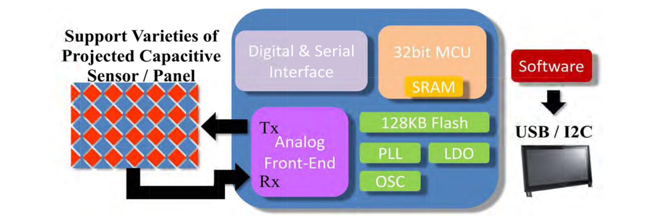
Figure 1 SiS9527 Touch System Diagram
Features
- Mutual Capacitive Sensing Technology
- High Performance Driving and Sensing Engine
- 12bit ADC
- SiS9527 AFE with up to 96 RX Channels and up to 60 TX Channels
- Frame-based Hardware Sensing Engine
- Dynamic Report Rate: TBD
- Internal low power OSC
- Build-in LDO for Sensing Engine
- RF immunity and Power Noise Immunity
- 10 Fingers Multi-Touch Support
- Host Interface
- Support I2C-compatible slave Interface
- Support USB
-Operation Core/IO Voltage - OVDD33 and AVDD33 Voltage: 3.3V
- I2C Interface I/O Voltage: 1.8V & 3.3V
- Palm Rejection
- Water proof
- Green Package
- RoHS compliance & Halogen Free, 215pin BGA 11mmx11mm
Pin Description
Sensor Interface
| Pin Name | Pin No. | Pin Name | Pin No. | Pin Attr | Description |
|---|---|---|---|---|---|
| TX1 | Y20 | TX31 | W11 | Out | Drive signal output pin |
| TX2 | AA20 | TX32 | Y11 | ||
| TX3 | W19 | TX33 | AA11 | ||
| TX4 | Y19 | TX34 | W10 | ||
| TX5 | AA19 | TX35 | Y10 | ||
| TX6 | W18 | TX36 | AA10 | ||
| TX7 | Y18 | TX37 | W9 | ||
| TX8 | AA18 | TX38 | Y9 | ||
| TX9 | V17 | TX39 | AA9 | ||
| TX10 | W17 | TX40 | W8 | ||
| TX11 | Y17 | TX41 | Y8 | ||
| TX12 | AA17 | TX42 | AA8 | ||
| TX13 | V16 | TX43 | W7 | ||
| TX14 | W16 | TX44 | Y7 | ||
| TX15 | Y16 | TX45 | AA7 | ||
| TX16 | AA16 | TX46 | W6 | ||
| TX17 | V15 | TX47 | Y6 | ||
| TX18 | W15 | TX48 | AA6 | ||
| TX19 | Y15 | TX49 | W5 | ||
| TX20 | AA15 | TX50 | Y5 | ||
| TX21 | V14 | TX51 | AA5 | ||
| TX22 | W14 | TX52 | W4 | ||
| TX23 | Y14 | TX53 | Y4 | ||
| TX24 | AA14 | TX54 | AA4 | ||
| TX25 | W13 | TX55 | Y3 | ||
| TX26 | Y13 | TX56 | AA3 | ||
| TX27 | AA13 | TX57 | Y2 | ||
| TX28 | W12 | TX58 | AA2 | ||
| TX29 | Y12 | TX59 | Y1 | ||
| TX30 | AA12 | TX60 | AA1 |
| Pin Name | Pin No. | Pin Name | Pin No. | Pin Name | Pin No. | Pin Attr | Description |
|---|---|---|---|---|---|---|---|
| RX1 | L3 | RX33 | C4 | RX65 | B12 | In | Sense signal input pin |
| RX2 | L2 | RX34 | B4 | RX66 | C12 | ||
| RX3 | L1 | RX35 | A4 | RX67 | A13 | ||
| RX4 | K3 | RX36 | C5 | RX68 | B13 | ||
| RX5 | K2 | RX37 | B5 | RX69 | D13 | ||
| RX6 | K1 | RX38 | A5 | RX70 | C13 | ||
| RX7 | J1 | RX39 | C6 | RX71 | A14 | ||
| RX8 | J2 | RX40 | B6 | RX72 | B14 | ||
| RX9 | J3 | RX41 | D6 | RX73 | D14 | ||
| RX10 | H1 | RX42 | A6 | RX74 | C14 | ||
| RX11 | H2 | RX43 | C7 | RX75 | A15 | ||
| RX12 | H3 | RX44 | A7 | RX76 | B15 | ||
| RX13 | G1 | RX45 | B7 | RX77 | D15 | ||
| RX14 | G2 | RX46 | D7 | RX78 | C15 | ||
| RX15 | G3 | RX47 | D8 | RX79 | A16 | ||
| RX16 | F1 | RX48 | C8 | RX80 | B16 | ||
| RX17 | F2 | RX49 | A8 | RX81 | A17 | ||
| RX18 | F3 | RX50 | B8 | RX82 | C16 | ||
| RX19 | E1 | RX51 | D9 | RX83 | B17 | ||
| RX20 | E2 | RX52 | C9 | RX84 | A18 | ||
| RX21 | E3 | RX53 | A9 | RX85 | C17 | ||
| RX22 | D1 | RX54 | B9 | RX86 | A19 | ||
| RX23 | D2 | RX55 | D10 | RX87 | B18 | ||
| RX24 | D3 | RX56 | C10 | RX88 | C18 | ||
| RX25 | C2 | RX57 | A10 | RX89 | A20 | ||
| RX26 | C1 | RX58 | B10 | RX90 | B19 | ||
| RX27 | C3 | RX59 | A11 | RX91 | B20 | ||
| RX28 | B1 | RX60 | B11 | RX92 | A21 | ||
| RX29 | B2 | RX61 | C11 | RX93 | B21 | ||
| RX30 | A2 | RX62 | D11 | RX94 | C19 | ||
| RX31 | B3 | RX63 | D12 | RX95 | C21 | ||
| RX32 | A3 | TX60 | AA1 | RX96 | C20 |
USB Interface
| Pin Name | Pin No. | Pin Attr | Description |
|---|---|---|---|
| USB- | G20 | In/Out | USB Data- |
| USB+ | G21 | InOut | USB Data+ |
I2C Interface
| Pin Name | Pin No. | Pin Attr | Description |
|---|---|---|---|
| INT | T3 | Out | USB Data-Interrupt pin sending request to HOST |
| I2C_CLK | T2 | In/Out | I2C serial clock input/output |
| I2C_DA | T1 | In/Out | I2C seral data input/output |
GPIO Interface
| Pin Name | Pin No. | Pin Attr | Description |
|---|---|---|---|
| GPIO0 | U1 | In/Out | General purpose input/output port |
| GPIO1 | U2 | In/Out | General purpose input/output port |
| GPIO2/TP_ID0 | U3 | In/Out | General purpose input/output port |
| GPIO3/TP_ID1 | V1 | In/Out | General purpose input/output port |
| GPIO4/UART_RX | V2 | In/Out | General purpose input/output port |
| GPIO5/UART_TX | V3 | In/OUT | General purpose input/output port |
Pin Description
| Pin Name | Pin No. | Pin Attr | Description |
|---|---|---|---|
| A0/CID0 | N20 | In/Out | Chip ID Pin / Channel select address |
| A1/CID1 | M19 | In/Out | Chip ID Pin / Channel select address |
| A2/CID2 | M20 | In/Out | Chip ID Pin / Channel select address |
| A3/CID3 | L21 | In/Out | Chip ID Pin / Channel select address |
| A4/CID4 | L20 | In/Out | Chip ID Pin / Channel select address |
| A5 | K20 | Out | Output channel select address |
| A6 | K21 | Out | Output channel select address |
| OE_1 | P20 | Out | Output enable |
| OE_2 | N22 | Out | Output enable |
| R_DIN | R20 | ||
| COUT | J21 | ||
| CLK | J20 | Out | Chanel select clock |
| HVRSTN | P21 | Out | |
| RESET# | R21 | In | Low activ power on reset signal |
Power and Ground Signals
| Pin Name | Pin No. | Pin Attr | Description |
|---|---|---|---|
| C1P | Y21 | PWR | Connect to external capacitor |
| C1N | AA21 | PWR | Connect to external capacitor |
| C2P | W21 | PWR | Connect to external capacitor |
| C2N | W20 | PWR | Connect to external capacitor |
| C3P | V21 | PWR | Connect to external capacitor |
| C3N | V20 | PWR | Connect to external capacitor |
| C4P | U21 | PWR | Connect to external capacitor |
| C4N | U20 | PWR | Connect to external capacitor |
| HVDD | T20 | PWR | Connect to external capacitor |
| CHVDD | T21 | PWR | Connect to external capacitor |
| DVSS | M1,M2,M3 | Digital 0V | Ground |
| TP18 | N1 | MAIN | |
| OVDD33 | F20 | Digital 3.3V | MAIN |
| TP12 | H20 | MAIN | |
| SPIMSCS0 | R1 | In | SPI slave chip select |
| SPIMSCS1 | R2 | In | SPI slave chip select |
| SPIMSCS2 | R3 | In | SPI slave chip select |
| SPIMISO | P2 | Out | SPI Slave mode data output |
| SPIMOSI | N2 | In | SPI Slave mode data input |
| SPIMSCK | P1 | In | SPI serial clock input |
| LVSS | W1,W2,W3 | Digital 0V | Ground |
| AVSS | D20,D21 | Analog 0V | Ground |
| TP28_1 | E20 | analog power | MAIN |
| TP28_2 | E21 | analog power | MAIN |
| AVDD33 | F21 | Analog 3.3V | MAIN |
| OSCIN | H21 | In | Oscillator input |
| NC | N3,P3 | - | - |
Electrical Characteristics
Absolute Maximum Ratings
Table 1 shows SIS9527 stress ratings only. Extended exposure to the maximum ratings might degrade device reliability. Although SIS9527 has protective circuitry to resist damage from electrostatic discharge (ESD), precautions should always be taken to avoid high voltage or electric field.
| Symbol | Parameter | Min | Max | Unit | Notes |
|---|---|---|---|---|---|
| Tstorage | Storage Temperature | -40 | 90 | °C | |
| Ta | Ambient Operating Temperature | -40 | 85 | °C | |
| OVDD33 AVDD33 | 3.3V Supply Voltage | -0.3 | 3.6 | V |
DC Characteristics
OVDD33 = 3.3V
AVDD33 = 3.3V
AVSS = LVSS = DVSS = GND = 0V
| For 3.3V I/O | ||||
|---|---|---|---|---|
| Symbol | Parameter | Min | Typ | Max |
| Vil (V) | Input low voltage | 0.8 | ||
| Vih (V) | Input high voltage | 2.0 | ||
| Vol (V) | Output low voltage | 0.4 | ||
| Voh (V) | Output high voltage | VDDIO-0.4 | ||
| Iil (uA) | Input leakage current | -10 | +10 | |
| Ihiz (uA) | Output tri-state leakage current | -10 | +10 | |
| Pull-up (kohm) | Internal Pull-up resistor | 39 | ||
| Pull-down (kohm) | Internal Pull-down resistor | 39 |
Packing Information
| Not take off the seal ( Al Bag ) | Take off the seal ( Al Bag ) | ||||
|---|---|---|---|---|---|
| Preserved conditions | Storage life | General Preserved conditions | Storage life | ||
| Temperature | Humidity | Temperature | Humidity | ||
| 0~40 °C | < 90 %RH | 12 Months | 25±5 °C | < 60 %RH | 168 Hours |
Product Reliability
| Test Item | Spec. |
|---|---|
| ESD | HBM: >2000V |
| MM: >200V | |
| CDM: >1000V |
Power Consumption Information
| Mode | Power Current | Note |
|---|---|---|
| Normal Operation Mode | 59 mA @ Max. | |
| Idle Mode | 32 mA | |
| Sleep Mode | 6.3 mA |
Power Sequence
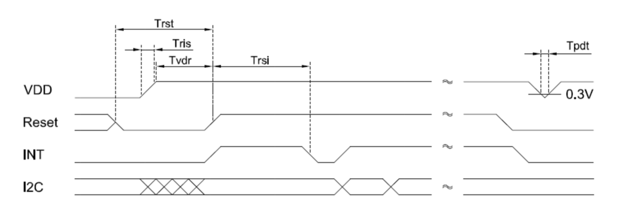
| Parameter | Description | Min | Max | Units |
|---|---|---|---|---|
| Tris | VDD power on Rise time from 0.1VDD to 0.9VDD | - | 2 | ms |
| Tpdt | VDD Power off lower than 0.3V Interval | 5 | - | ms |
| Tvdr | VDD power on at 3.3V to RESET# at 2.0V | 5 | - | ms |
| Trsi | Time of starting to report point after resetting | 100 | - | ms |
| Trst | Reset time | 5 | - | ms |
I2C Interface
| Vendor | SiS |
| Slave Address | 0x5c(7-bits addressing, programmable) |
| Clock rate | @400 kHz (fast mode) |
| Interrupt mode | Default active low, level trigger |
| _CID | PNP0C50 |
| _DSM | 3CDFF6F7-4267-4555-AD05-B30A3D8938DE |
| HID Descriptor address | 0x0000 |
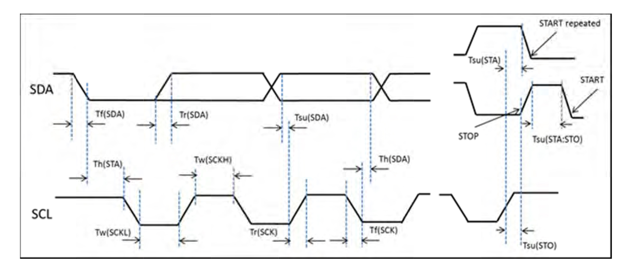
| Symbol | Parameter | SCL=100KHz | SCL=400KHz | Unit | ||
|---|---|---|---|---|---|---|
| Min | Max | Min | Max | |||
| Tw(SCLH) | SCL clock high time | 4.7 | 1.3 | us | ||
| Tw(SCLL) | SCL clock low time | 4.0 | 0.6 | |||
| Tsu(SDA) | SDA setup time | 250 | 100 | ns | ||
| Th(SDA) | SDA data hold time | 0 | 0 | 900 | ||
| Tr(SDA)Tr(SCL) | SDA&SCL rise time | 1000 | 300 | |||
| Tf(SDA)Tf(SCL) | SDA&SCLA fall time | 300 | 300 | |||
| Th(STA) | Start condition hold time | 4.0 | 0.6 | us | ||
| Tsu(STA) | Repeated Start condition setup time | 4.7 | 9.6 | |||
| Tsu(STO) | Stop condition setup time | 4.0 | 0.6 | |||
| Tw(STO:STA) | Stop to Start condition time(bus free) | 4.7 | 1.3 |
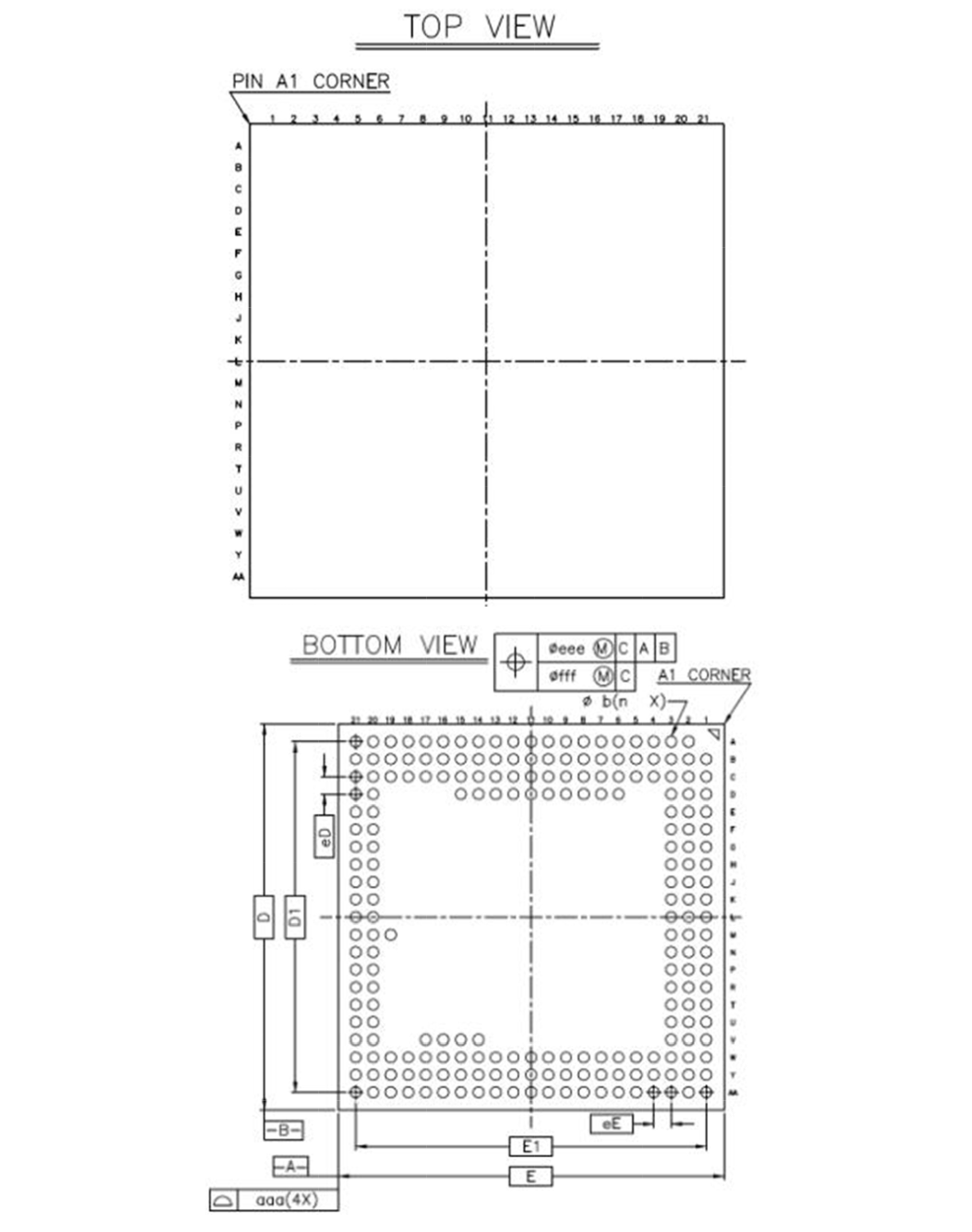
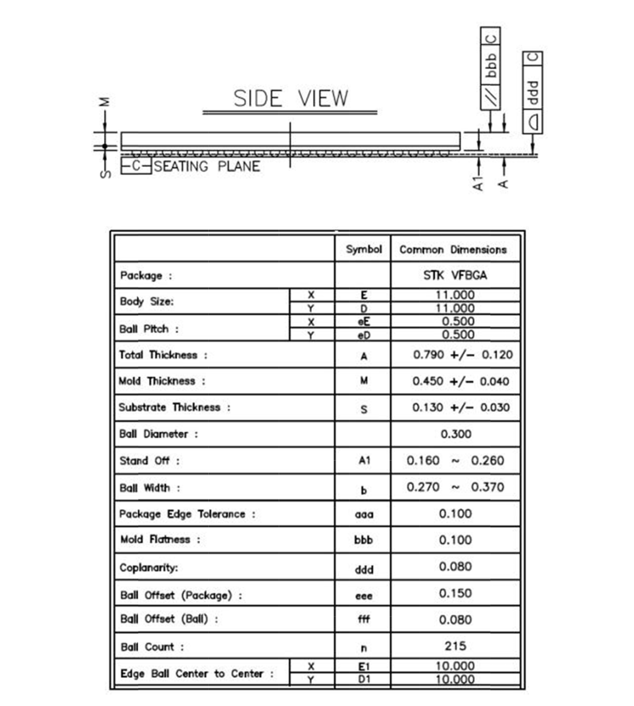
Mechanical Dimension
Application Circuit
SiS9527 Reference Circuit
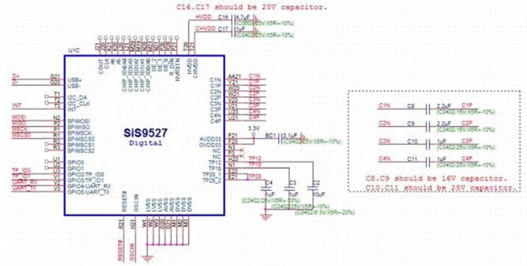
| Item | Symbol | Value | Part NO. | Quantity | Package |
|---|---|---|---|---|---|
| 1 | U1 | - | SiS9527 | 1 | |
| 2 | C2,C3,C4,C10,C11,C17 | 1uF/25V/X5R+-10% | - | 6 | 0402 |
| 3 | C9,C8 | 2.2uF/16V/X5R+-10% | - | 2 | 0402 |
| 4 | C16 | 4.7uF/25V/X5R+-10% | - | 1 | 0402 |
| 5 | BC1 | 0.1uF/25V/X5R+-10% | - | 1 | 0402 |
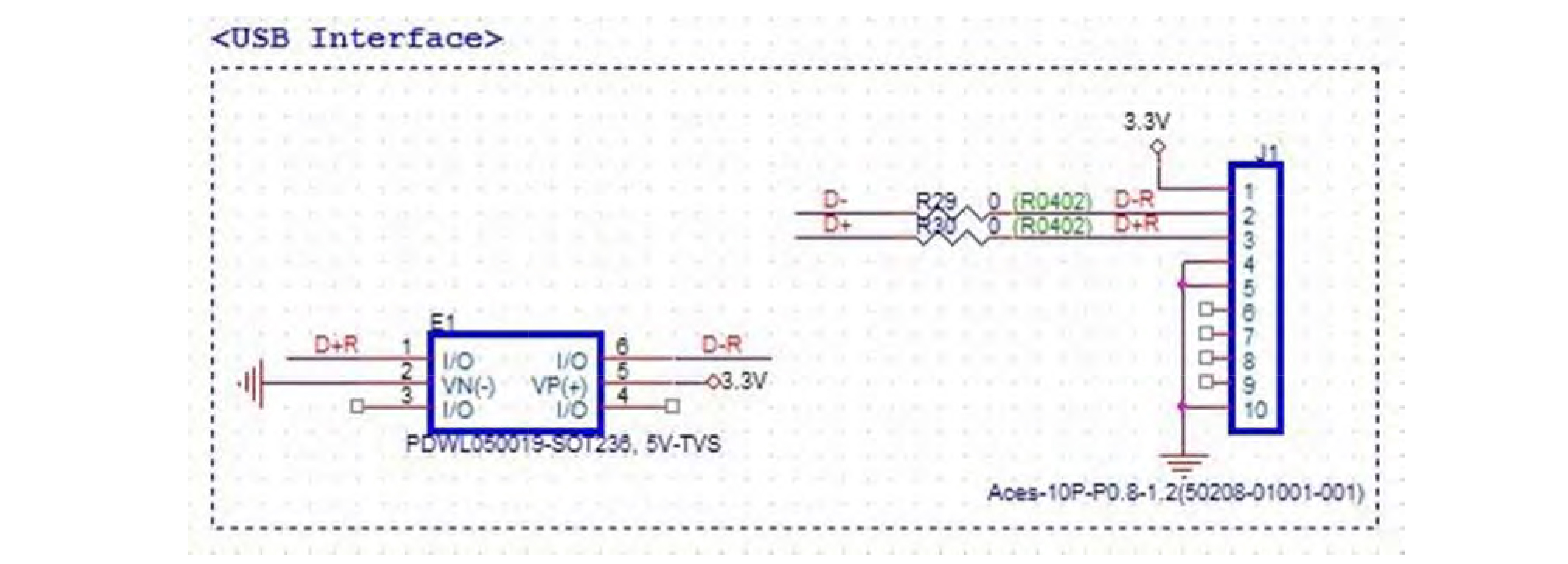
USB and I2C Circuit
| Item | Symbol | Value | Part NO. | Quantity | Package |
|---|---|---|---|---|---|
| 1 | E1 | 5V-TVS | PDWL050019 | 1 | SOT236 |
| 2 | J1 | Aces-6P-P0.6-(50376) | - | 1 | |
| 3 | R29,R30 | 0R | - | 2 | 0402 |
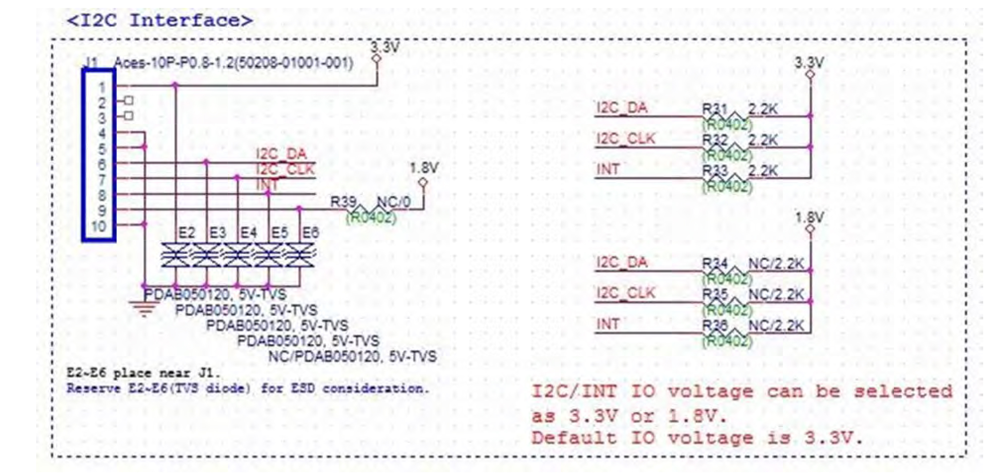
| Item | Symbol | Value | Part NO. | Quantity | Package |
|---|---|---|---|---|---|
| 1 | E2,E3,E4,E5,E6 | 5V-TVS | PDAB050120 | 5 | SOT236 |
| 2 | J1 | Aces-10P-P0.8-1.2 | - | 1 | |
| 3 | R31,R32,R33 | 2.2K | - | 3 | 0402 |
OSC Circuit
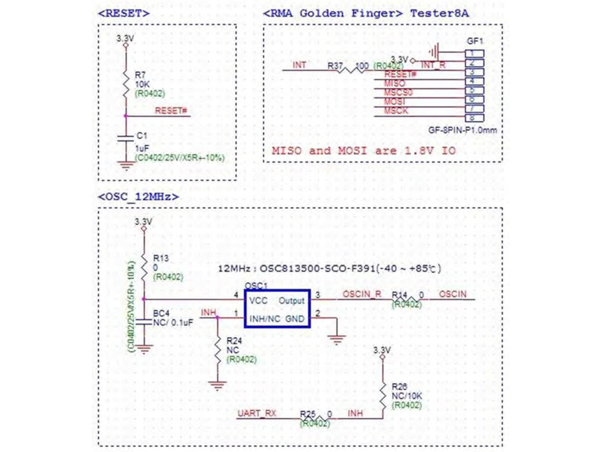
| Item | Symbol | Value | Part NO. | Quantity | Package |
|---|---|---|---|---|---|
| 1 | R7 | 10K | - | 1 | 0402 |
| 2 | C1 | 1uF/25V/X5R+-10% | - | 1 | 0402 |
| 3 | R37 | 100R | - | 1 | 0402 |
| 4 | OSC15 | 12MH | OSC813500-SCO-F391 | 1 | |
| 5 | R13,R14,R25 | 0R | - | 3 | 0402 |
